On the hub page I called rev 1 a “zero-thought design.” That’s not quite right. Zero-thought would mean flipping a coin on every choice. What I did was pick the mistakes I think I can attribute, and follow best practice everywhere else.
The point of the project is to measure noise on a deliberately broken board, tie each noise source back to a specific design choice, and fix them one at a time across revisions. That only works if the broken parts are the ones I can isolate. Breaking everything at once would give me a noisy board with too many overlapping causes to untangle.
So rev 1 has a curated set of antagonists, plus a small set of knobs I can turn without a respin. Here’s what’s on it.
The ADC#
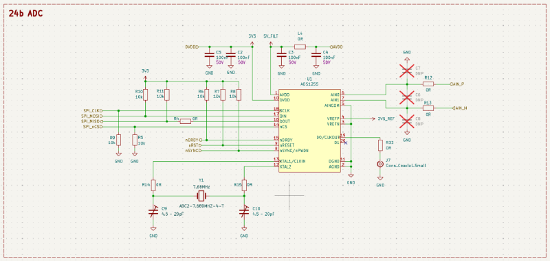
The ADC is a TI ADS1255 — 24-bit, single differential channel, 4th-order delta-sigma, up to 30 kSPS, with a programmable gain amplifier up to 64x. I picked it mostly because I’ve used it before and didn’t want the ADC itself to be the thing I was learning. The PGA and sample-rate flexibility are a bonus: both give me knobs to sweep when I’m measuring, which means I can characterize how the gain stage and the digital filter shape interact with each noise source, not just measure them at a single operating point.
The host#
There’s no MCU on this board. The SPI bus is brought out to a header and connects to an STM32 Nucleo-F303RE sitting next to the board on the bench. UART off the Nucleo for data.
This is the kind of choice that looks like cheating in a “deliberately bad design” project, because the canonical advice is to keep the digital processor away from the ADC, and I’ve done that for free by putting the processor on a different PCB. The reason is BOM and project scope, not isolation hygiene — I didn’t want to populate and bring up an MCU subsystem when I’m trying to learn about analog noise, and I had Nucleos on the shelf.
An on-board MCU and an on-board SMPS aren’t interchangeable noise antagonists. They couple differently — the SMPS is mostly conducted noise on the supply rail with some radiated content from the inductor; an MCU adds ground bounce, broadband activity from data toggling, and clock harmonics radiated from traces. “I broke the regulator” and “I put the MCU next to the ADC” would teach different lessons. For rev 1 the SMPS is the headline antagonist and that’s enough.
Power — the headline mistake#
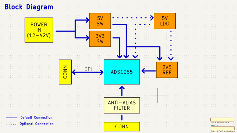
12V comes in on a barrel jack. Three regulators on the board: a 3.3V SMPS for digital, a 5V SMPS, and a 5V LDO. For rev 1 the 5V SMPS feeds everything on the analog side — AVDD, the reference circuit, the lot. This is the design choice I most expect to dominate the noise floor.
The interesting bit is the way I’ve built in the next revision without respinning. There are shorting resistors that let me reroute the analog 5V from the SMPS to the LDO. When I do that, I’ll also reconfigure the 5V SMPS to 5.25V and feed it into the LDO as a preregulator, so the LDO has enough headroom. The switchover is two resistor moves on the bench.
That gives me a clean A/B: same board, same layout, same parasitics, only the regulator changes. Whatever the noise floor does between those two configurations is attributable to the regulator with reasonable confidence. If I’d put the LDO on rev 1 instead, I’d be comparing two different boards and arguing about whether the layout differences mattered.
The reference#
The reference is a voltage divider off the analog 5V rail, buffered by an OPA356 op-amp, exactly as the ADS1255 datasheet suggests. Nothing creative here — the datasheet circuit is the datasheet circuit.
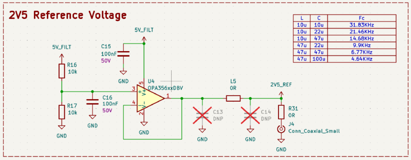
What I did add is unpopulated low-pass filter footprints on both the reference output and the ADC input. They’re empty for rev 1. They exist so that when I’m chasing a noise contribution I think might be on the reference, I can populate a filter and remeasure without a board spin. Same logic as the LDO shorting resistors: build the knob now, turn it later.
Ground and stackup#
Single solid ground across all four layers. Stackup is signal / ground / ground / signal. Both are best practice.
I went with best practice here for the same reason I put the MCU off-board: I couldn’t see how I’d validate the alternative cleanly. A split plane done wrong is a real failure mode, but to attribute noise to it I’d need a board with the split and one without, which is a whole extra revision for one variable. Same for the stackup. The mistakes I picked were ones I thought I could isolate with the tools I have on the bench. Ground topology didn’t make that list.
That might be the wrong call. It’s possible the most instructive thing I could have done was screw up the grounding and watch what happened. I’ll come back to that if the measurements suggest I should.
Physical#
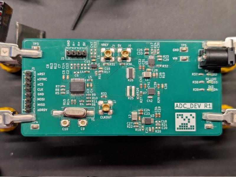
Four layers, roughly 120 × 80 mm. Inputs are 0.1" headers — nothing fancy, no SMAs on the signal path. There are MCX test points on the analog 5V rail, the ADC clock-out pin, and the reference voltage, so I can probe those three without dragging clips around.
What rev 1 is and isn’t#
Rev 1 is one deliberate mistake (SMPS on analog), a couple of unpopulated knobs (the LDO switchover and the filter pads), and best practice everywhere else. It’s not a worst-case board. It’s the smallest perturbation away from a reasonable board that I think I can attribute and measure. Next set is to get data from the board.
The schematics and layout can be found on my Codeberg