I hit what looked like a bug in my ADC driver and spent longer than I’d like chasing it. There was no bug. The part was doing exactly what it should with floating inputs does. This is the writeup so the next person — probably me — recognizes it faster.
I was finishing the helper functions and started testing the function that reads the ADC code. The values were strange. Run to run, the starting value was effectively random: one run would sit around 680k, the next around -3M. On top of that there was what I took for noise.
My first instinct was timing or my calibration routine. I was fairly sure the SPI layer was fine, very read and write I traced made sense, and registers read back what I’d written. So I kept poking at the code that felt most likely to be subtly wrong, calibration and timing, and got nowhere. Nothing there was wrong. Eventually I plotted the output instead of reading numbers off the console. That’s when it cleared up.
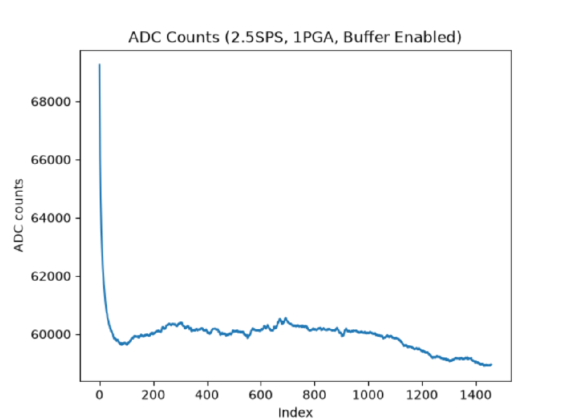
ADC code over time with the input floating. The slow wander is the tell.
The shape was familiar. It’s what a buffer does when its inputs are floating. I had nothing connected to the input and I was enabling the high-impedance buffer. So there was no signal to read — what I was actually seeing was the input bias current charging the amplifier’s input impedance, plus stray parasitics from the ADC pin to the board. With no source connected, the bias current has no defined path, so it accumulates on whatever capacitance is present and the node drifts. That accounts for the wander and the noise. It doesn’t account for the random starting value — why one run begins near 680k and the next near -3M. My guess is residual charge left on the node between power cycles, but I haven’t confirmed it, so I’m leaving it as a loose end rather than dressing it up as an explanation.
The useful part was fixing my mental model. I’d been thinking of the input impedance as a resistor: one big number that lightly loads the input. It isn’t. It’s a frequency-dependent impedance — a high resistance (10⁵ to 10¹² Ω) in parallel with a small shunt capacitance (up to ~25pF), per ADI’s MT-040. Differential impedance between the two inputs, common-mode impedance from each input to ground. Once you picture it as an R‖C instead of an R, “bias current slowly charging a capacitor” stops being a mystery and becomes the obvious thing for the circuit to do.
With that model I built a rough LTspice version — the same R‖C network with a small current driven into it — and got a differential voltage with a shape close to the measured ADC plot. Not a fit, just enough to confirm I had the mechanism right.
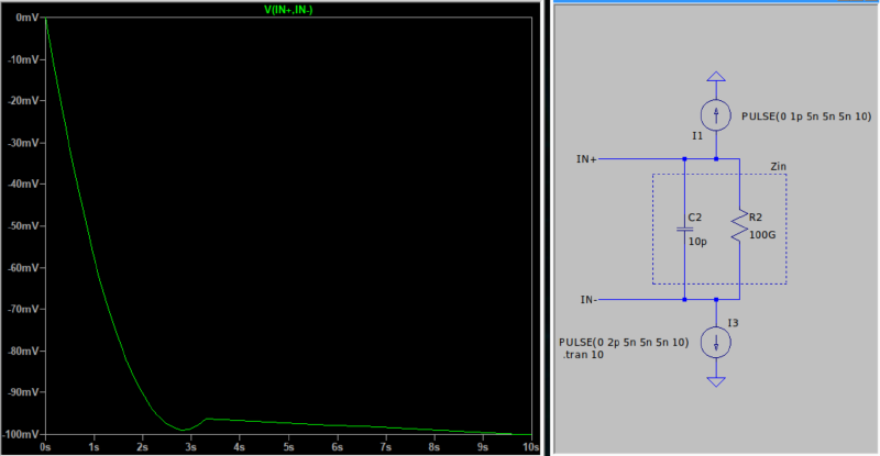
The R‖C input model and its output. Compare the curve to the ADC plot above.
There was never a bug. Disabling the buffer, or connecting a low-impedance sensor to the input, gives the bias current somewhere to go and the reading settles. The driver was fine the whole time. What I was missing is that “nothing connected” is not the same as “zero input” when the front end is a high-impedance buffer — it’s an open invitation for the bias current to do exactly this.