Streaming the ADS1255 at 30kSPS: A DMA Modification#
The last post in this series left me with an open question: the ADS1255 driver worked, but I could only read at the lower end of its available data rate. The ADS1255’s actual ceiling is 30,000 samples a second, and I was pretty sure I wasn’t going to hit that target with what I’d built. Thirty thousand samples a second means a new 24-bit conversion every 33 µs.
33 microseconds, three jobs#
Getting one sample from the ADC to my PC within 33µs requires three things:
- read 24 bits of SPI data off the ADC
- attach an 8-bit CRC (generated by the STM32’s CRC peripheral)
- transmit the resulting 4 bytes over UART with standard 8N1 framing, for a total of 40 bits
The math that killed the easy version#
My first move was to check whether plain blocking HAL_SPI_Receive and HAL_UART_Transmit could do it. The ADS1255’s SPI ceiling is 1.9 Mbps, so the best case scenario for a 24-bit read is 24 / 1.9 MHz ≈ 12.6 µs. I measured the actual SPI call overhead by capturing the cycle counter before and directly after the call:
uint32_t t0, t1;
t0 = DWT->CYCCNT;
HAL_SPI_Receive(ads->hspix, spiRx, 3, 10);
t1 = DWT->CYCCNT;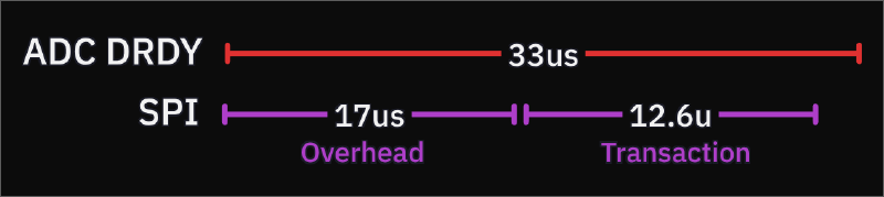
Consistently, about 17 µs on top of the 3-byte SPI transfer itself, so a single SPI operation takes 29.6 µs. The remaining 3.4 µs would need a UART clock around 11.8 Mbps with nothing held in reserve. Blocking calls were never going to work, at any SPI speed I could reasonably reach. Time to learn DMA.
DMA doesn’t make the wire faster#
I’d heard of DMA before, but never really spent any time learning how it actually works. What DMA buys me is CPU time. Using DMA the peripheral moves data to or from memory on its own, instead of the CPU waiting on a status flag to say the data’s ready. That’s only useful if the CPU has something worthwhile to do with the freed-up time, and in my case it does. While UART is transmitting sample N, the CPU can set up the SPI DMA to read sample N+1.
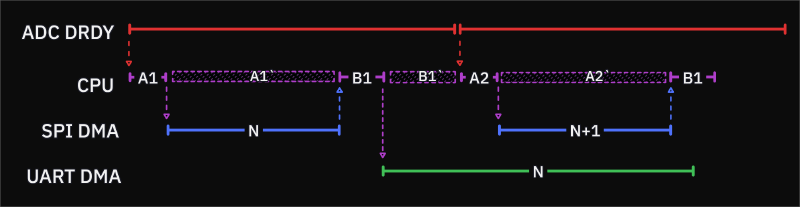
A1 is the SPI DMA arm overhead, and A1’ is the CPU time it frees up while that transfer runs. B1 covers the SPI callback and the UART DMA arm overhead, B1’ is the free’ed up time again, and A2 is the SPI arm overhead for the next read. C, running underneath, is UART actually transmitting sample N.
This led into a second concept I wasn’t familiar with. Double buffering, as the name implies, needs two data buffers. While SPI is writing sample N+1 to memory location B, UART is still reading sample N from memory location A.
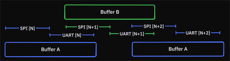
The swap happens in the SPI receive-complete callback. Whichever buffer SPI just filled gets pointed at the UART DMA, the SPI pointer advances to the other buffer, and the UART DMA is kicked off. Each time the receive-complete function runs, this shift repeats.
Almost fast enough#
Wiring up HAL_SPI_Receive_DMA and HAL_UART_Transmit_DMA and chaining the callbacks got samples moving. The DMA setup overhead measured around 13.6 µs. Turning on -Os dropped that to roughly 7 µs, the single biggest overhead win I got without changing a single line of code.
That’s great, but it still wasn’t enough. At the MCU’s default 72 MHz, the closest SPI clock speed I can get without going over the ADS1255’s 1.9 MHz ceiling is 1.125 MHz. 24 bits at 1.125 MHz is 21.3 µs, add the 7 µs arm overhead and that’s 28.3 µs before UART even starts. That didn’t leave much of the 33 µs budget for UART, and 28.3µs wasn’t a margin I felt comfortable with.
An accidental command#
While chasing the rest of that overhead, DRDY started doing something new. Instead of a clean periodic DRDY pulses, the DRDY would behave chaotically, or stop all together, with no pattern I could find on the scope. I traced it to something I hadn’t known about SPI. In 2-line master mode, HAL_SPI_Receive_DMA doesn’t actually do a receive-only transfer, it internally calls HAL_SPI_TransmitReceive_DMA(hspi, pData, pData, Size), using the same pointer for both directions. Generating the SPI clock in master mode apparently requires something shifting out the TX side, so a receive still needs a transmit alongside it, and HAL’s answer is to reuse the RX buffer as disposable TX content. I’m not fully sure why clock generation is tied to TX specifically rather than being free-running, and I didn’t chase it further once the fix worked.
The problem is what’s sitting in that buffer, the previous sample’s ADC reading, clocked back out to the ADC’s as if it were a command byte. Most of the time that’s harmless garbage the ADS1255 ignores. But once the ADC is calibrated and the input sits near zero, the reading hovers around zero too. Small positive codes put the least significant byte in 0x00–0x0F, small negative codes (two’s complement) put it in 0xF0–0xFF. Most of the ADS1255’s actual commands live in exactly those two ranges, so a stale, near-zero sample is a lot more likely to accidentally spell out a real command than a stale reading from anywhere else in its range would be.
The fix was to set the TX buffer, in my custom function, to a fixed known-safe value instead of reusing the live RX pointer. That way the ADC never sees anything on its command input during a read except bytes it’s guaranteed to ignore.
Do it once, not every time#
While turning on -Os cut down my SPI DMA overhead by almost half, I still needed to write my own DMA handler to deal with the edge case above, so I figured I’d try to squeeze out a bit more margin while I was in there.
Rewriting that function meant reading HAL’s SPI DMA handler line by line. Most of what it does on every call is the same:
- set callback function pointers
- set a couple of
CR2bits - set the RX byte limit
None of these parameters change between ADC reads, so they can be moved into a one-time init function that runs before streaming starts. All that’s left per call is re-enabling the DMA stream/channel with HAL_DMA_Start_IT, and clearing whatever status flags carried over from the last transfer. All in all, that took the DMA overhead from ~7 µs down to about 4.7 µs, almost a third of where I started at 13.6 µs.
Chasing 1.9 MHz#
I need to speed up the SPI transfer. Working backwards from the ADC’s 1.9 MHz ceiling, I land on two usable prescalers, 32 and 16, giving a system clock of ~60.8 MHz or ~30.4 MHz. There’s no reason to run the MCU slower, so 60 MHz is the clear choice. That puts the SPI clock at 1.875 MHz (60 MHz / 32), and 24 bits at 1.875 MHz is 12.8 µs.
This takes my total SPI transfer time, from DRDY to when UART takes over, to 17.5µs (4.7µs + 12.8µs), down from the blocking version’s 29.6µs.
Passing the baton#
The SPI callback checks whether the previous UART operation has completed. If not, it loops in place and waits, making the callback a blocking operation. That’s a necessary check, if the callback skipped the UART because it was busy, that sample would be lost. UART runs at 2Mbaud, a standard rate independent of the SPI clock. Four bytes at 8N1 is 40 bits, 20µs of transfer. I timed the UART handoff the same way as the SPI call, cycle counter at the DMA call, cycle counter at the callback, and got about 28µs total, transfer plus roughly 8µs of arm overhead. So long as that stays under 33µs, UART should never run through more than one DRDY, and I shouldn’t miss a sample.
1M sample test#
To see if this actually holds up and not just in a quick bench test, I set the ADC to 30kSPS and ran it for 1,000,000 samples, about three seconds of continuous streaming at full rate. I used stty to capture the raw UART output to a text file, then wrote a small Python script to split it into 4-byte packets and check each CRC against what the STM32 computed. All 1,000,000 packets passed, no CRC failures, no dropped bytes.
This is just one run on one board, I haven’t pushed past 1M samples or tried it under different conditions yet.
The code as it stands at the end of this post is tagged V2–DMA